Today I am putting out the first version of my KiCad via improvements. I created this during routing of my Nokia Retro Fit project. The board I wanted to create has this layer stack:
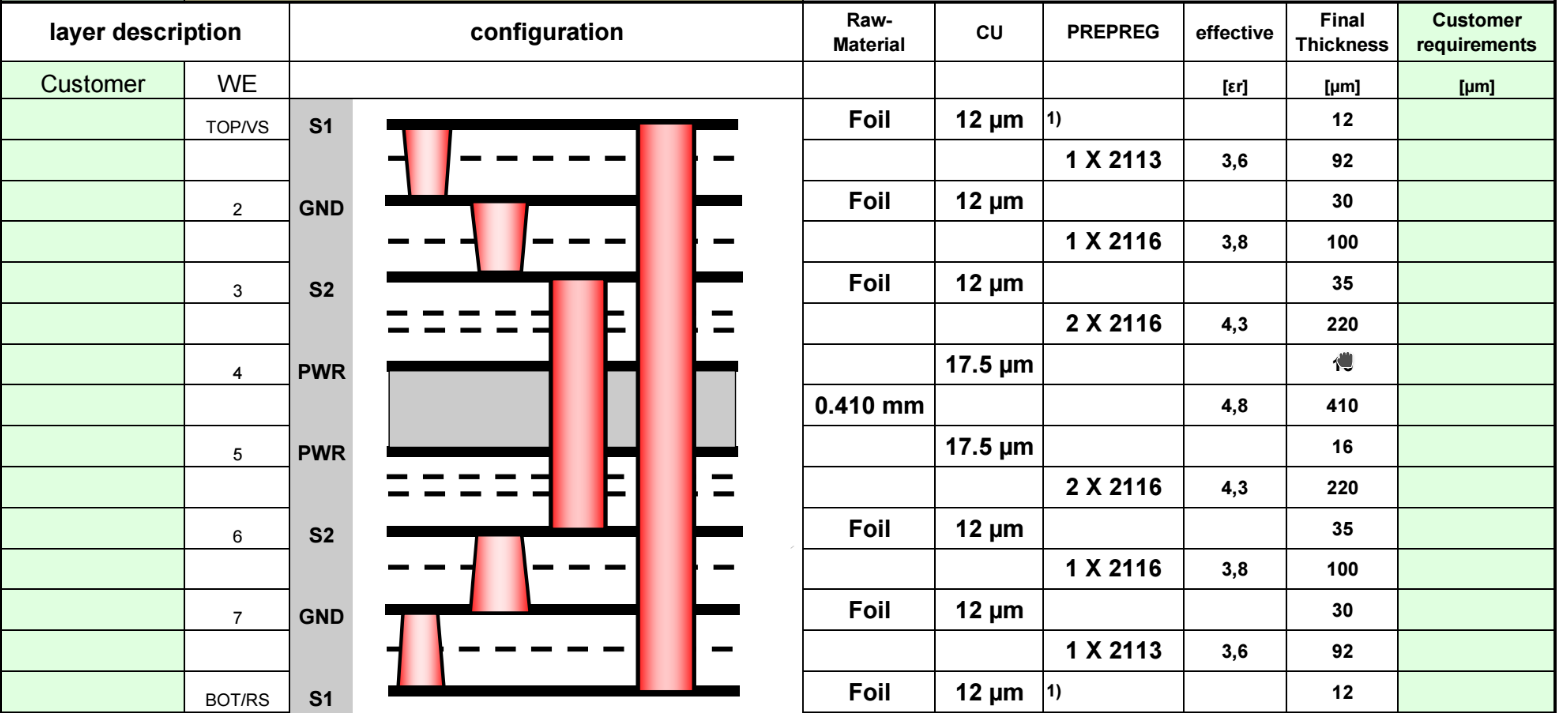
As you can see I want to be able to create micro vias on the layers 1,2,3 and 6,7,8. Using even the nightly builds of KiCad only allows you to place micro vias on the top or bottom to the adjacent layer below. so from 1 to 2 and 7 to 8. This where my additions come into to play.
I enhanced the user vias diameter and drill part of the Design Rules dialog. It now comes with more options.
- Via Type (Through, Blind/Burried, Micro)
- Start Layer
- End Layer
The via class has those additional values as well.

Placing a micro vias during layout does not yet work as intended, but I am working on it. You can change it after placement nonetheless. So placing vias is not yet as comfortable as I would like it to be.
Editing a via after placing now gives you this dialog:
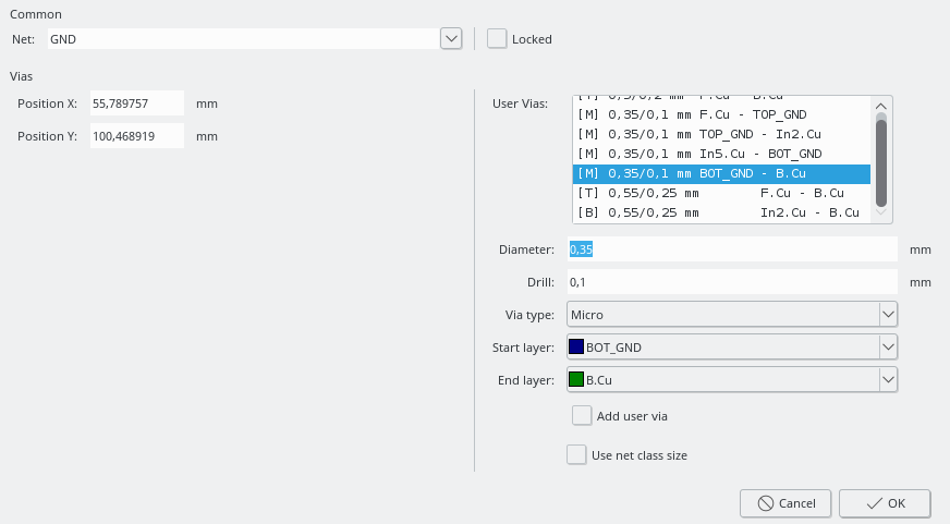
It gives you a list of all the vias created and you can double click to change the values below. It does not let you enter values that are not listed in the user via list. But you can select the „Add user via“ checkbox to add your desired values to the list of user vias.
With this modifications to the KiCad source code I think I should be able to finish routing my DDR3 signals.
The issue with measuring the tracks still is on my list of things to do. Placing micro vias in a sensible way was more important to achieve though.
To try out the changes for yourself you can find the source code here